

Dr. Yuan talks about diamonds: CVD cultivates diamonds for industrial use
Release time:
2021-06-30 00:00
Human beings have always hoped to cultivate diamonds for various industrial purposes. Up to now only the use of HPHT growth of small particles of diamond abrasive hardness, as a super hard material, made of a variety of grinding tools, used in grinding and polishing. However, in these aspects of acoustochemical electrothermal, a large area of single crystal diamond sheet material is required, which is still under development and is not really used.
It was first grown into polycrystalline diamond sheet or diamond film by CVD several decades ago. Because the surface is rough polycrystalline structure and difficult to polish, it has not been widely used. After about 2000, single crystal diamond began to grow in a new way. Single crystal CVD grown diamond is grown upward on flat sheet seed crystal sheet, which can make a large area, but its cost is too high to produce in large quantities, at a low enough price in the private industry applications. So it hasn't really been used in large numbers so far.
Our research direction:
1. Boron-containing CVD polycrystalline films and sheets are used as electrodes for water treatment, as water purification treatment, elimination of organic organisms and heavy metals in water, purification of precious metal tailings, desalination of seawater, extraction of valuable metals in seawater, decomposition of water into hydrogen and oxygen, and increase of voltage to separate a large amount of deuterium and tritium, which can be used as raw materials for nuclear fusion.
2, diamond heat plate, in high-power chips, electronic devices have great demand for heat dissipation, but now the price is too high, only military products have a small amount of demand, the price must be reduced to 1/10 of the current price, private products can afford.
3. Diamond LED ultrashort wave PN junction luminescence, diamond positive and negative semiconductors are grown on diamond wafers to produce 215nm LED luminescence, which is used as ultra-high power LED luminescence, production of sterilization tools, ultra-strong laser for cutting tools, long-distance killing weapons, and production of the most critical lithography light source in the semiconductor industry.
4, diamond wafer splicing CVD large-area single crystal wafer, as LED, semiconductor chip substrate, can completely solve the problem of heat dissipation and the use of a number of super excellent physical and chemical properties of diamond, will make the human semiconductor industry into the ultimate fourth generation of wafer materials, to solve the human use of silicon wafers has reached the limit of the problem.
The private use of CVD diamonds in industry will gradually develop and mature in the past few years, and the demand will be ten to a hundred times the share of jewelry diamonds. Cultivating diamonds, especially CVD diamonds, is now a mature sunrise enterprise. In the future, it will be used in jewelry diamonds and industrial heat dissipation, semiconductors, high-end electronics, auto-driving, quantum computers, high-end lasers... There is great room for development and it will be the beginning of a new era that will last for more than a hundred years.
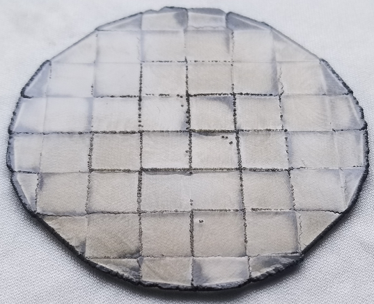
Single Crystal Diamond Splice Wafer
Related News
To participate in the "2011 Beijing International Lighting Exhibition" exhibition held in Beijing
Participate in the "7th Guangzhou International LED Exhibition (LED CHINA 2011)" exhibition held in Guangzhou
To participate in the "Japan International Electronic Products Exhibition" held in Tokyo, Japan"
Participated in the "Twelfth China International High-tech Achievement Fair" held in Shenzhen and won the "Excellent Product Award" certificate
Yuan Dong was invited to give a lecture at the Appraisal Institute of Taiwan Gemological Institute.
Dr. Yuan Zhizhong, Chairman of Bench Diamond Technology, gave a lecture entitled "Identification of Gem Diamonds Cultivated by CVD Method" at the Appraisal Institute on the 11.9 at the invitation of the Appraisal Institute of Taiwan Gemological Institute. In the lecture, Yuan Dong introduced in detail the historical principles of CVD diamonds and their development status, and introduced in detail several methods to distinguish CVD diamonds from natural diamonds on how to identify gem-grade CVD diamonds that participants are concerned about! Yuan Dong's wonderful speech was well received by the participants!
Yuan Dong Attends the Symposium at the Invitation of Hangzhou Jewelry City
Dr. Yuan Zhizhong, Chairman of Bench Diamond Technology, was invited by Hangzhou International Jewelry City to attend an academic symposium on November 19, 2013. At the symposium, Yuan Dong gave a speech entitled "International Situation and Identification of CVD Synthetic Diamonds" on the current situation of CVD synthetic diamonds that jewelers are concerned about and how to distinguish CVD diamonds from natural diamonds. In the speech, Yuan Dong introduced in detail the history of CVD diamonds, the international situation of CVD diamonds and the commonly used identification methods of CVD diamonds, and answered some questions raised by jewelers. Mr. Yuen's speech was well received by the participants, and all jewelers said they benefited.
Taidiam Technology (Zhengzhou) Co., Ltd.
Telephone:
Mailbox:
Address:
1-2 Floors, 9th Biulding, Henan Zhengzhou Export Processing Zone
Copyright©2023 Taidiam Technology (Zhengzhou) Co., Ltd. All Rights reserved |Business License| Label