

Products
Product Center
MengziFabrication of CVD Large Area Single Crystal Wafer by Diamond Wafer Splicing Method
Category:
MengziCVD industry
Product Description
A、Diamond wafer as LED, semiconductor chip substrate, can completely solve the problem of heat dissipation, diamond and a number of super excellent physical and chemical properties, will make the human semiconductor industry into the ultimate fourth generation of wafer materials.
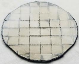
spliced diamond crystal
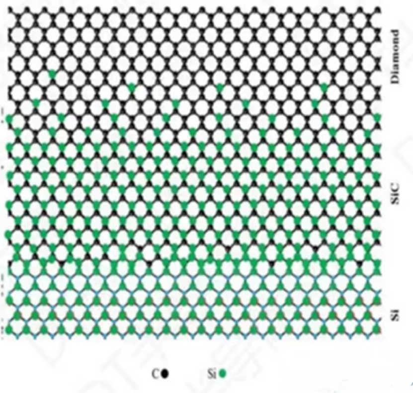
B、SOD Silicon on Diamond
Perfect diamond monocrystalline wafers are grown on 8-12 inch silicon wafers by ECR ALD from silicon decreasing and carbon increasing to replace silicon wafers as diamond wafers. Currently in research and development
Taidiam Technology (Zhengzhou) Co., Ltd.
Telephone:
Mailbox:
Address:
1-2 Floors, 9th Biulding, Henan Zhengzhou Export Processing Zone
Copyright©2023 Taidiam Technology (Zhengzhou) Co., Ltd. All Rights reserved |Business License| Label